- 您现在的位置:买卖IC网 > Sheet目录528 > UPA2211T1M-T1-AT (Renesas Electronics America)MOSFET P-CH 12V 8VSOF-SLIM
�� ��
��
��DATA� SHEET�
�MOS� FIELD� EFFECT� TRANSISTOR�
�μ� PA2211T1M�
�P-CHANNEL� MOS� FET�
�FOR� SWITCHING�
�DESCRIPTION�
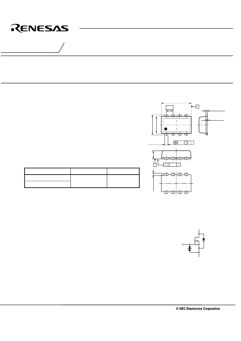
�PACKAGE� DRAWING� (Unit:� mm)�
�The� μ� PA2211T1M� is� P-channel� MOS� Field� Effect� Transistor� designed�
�for� power� management� applications� of� portable� equipments,� such� as�
�load� switch.�
�8�
�2.9� ±� 0.1�
�0.65�
�5�
�A�
�0.145� ±� 0.05�
�FEATURES�
�?� Low� on-state� resistance�
�R� DS(on)1� =� 25� m� Ω� MAX.� (V� GS� =� ?� 4.5� V,� I� D� =� ?� 7.5� A)�
�0� to� 0.025�
�R� DS(on)2� =� 34� m� Ω� MAX.� (V� GS� =� ?� 2.5� V,� I� D� =� ?� 3.8� A)�
�R� DS(on)3� =� 66� m� Ω� MAX.� (V� GS� =� ?� 1.8� V,� I� D� =� ?� 3.8� A)�
�?� Built-in� gate� protection� diode�
�?� ?� 1.8� V� Gate� drive� available�
�ORDERING� INFORMATION�
�0.32� ±� 0.05�
�S�
�1�
�4�
�0.05� M� S� A�
�0.05� S�
�1,� 2,� 3,� 6,� 7,� 8:� Drain�
�4� :� Gate�
�5� :� Source�
�PART� NUMBER�
�PACKING�
�PACKAGE�
�μ� PA2211T1M-T1-AT�
�μ� PA2211T1M-T2-AT�
�Note�
�Note�
�8� mm� embossed� taping�
�3000� p/reel�
�8-pin� VSOF� (1629)�
�0.011� g� TYP.�
�Note� Pb-free� (This� product� does� not� contain� Pb� in� external� electrode� and�
�other� parts.)�
�ABSOLUTE� MAXIMUM� RATINGS� (T� A� =� 25� °� C,� All� terminals� are� connected.)�
�Drain� to� Source� Voltage� (V� GS� =� 0� V)�
�Gate� to� Source� Voltage� (V� DS� =� 0� V)�
�V� DSS�
�V� GSS�
�?� 12�
�m� 8�
�V�
�V�
�EQUIVALENT� CIRCUIT�
�Drain� Current� (pulse)�
�Total� Power� Dissipation�
�Drain� Current� (DC)�
�Note1�
�Note2�
�Total� Power� Dissipation� (PW� =� 5� sec)�
�Note2�
�I� D(DC)�
�I� D(pulse)�
�P� T1�
�P� T2�
�m� 7.5�
�m� 30�
�1.1�
�2.5�
�A�
�A�
�W�
�W�
�Gate�
�Drain�
�Body�
�Diode�
�Channel� Temperature�
�Storage� Temperature�
�Notes� 1.� PW� ≤� 10� μ� s,� Duty� Cycle� ≤� 1%�
�T� ch�
�T� stg�
�150�
�?� 55� to� +150�
�°� C�
�°� C�
�Gate�
�Protection�
�Diode�
�Source�
�2.� Mounted� on� glass� epoxy� board� of� 25.4� mm� x� 25.4� mm� x� 0.8� mmt�
�Remark� The� diode� connected� between� the� gate� and� source� of� the� transistor� serves� as� a� protector� against� ESD.� When�
�this� device� actually� used,� an� additional� protection� circuit� is� externally� required� if� a� voltage� exceeding� the� rated�
�voltage� may� be� applied� to� this� device.�
�The� information� in� this� document� is� subject� to� change� without� notice.� Before� using� this� document,� please�
�confirm� that� this� is� the� latest� version.�
�Not� all� products� and/or� types� are� available� in� every� country.� Please� check� with� an� NEC� Electronics�
�sales� representative� for� availability� and� additional� information.�
�Document� No.� G19452EJ1V0DS00� (1st� edition)�
�Date� Published� September� 2008� NS�
�Printed� in� Japan�
�2008�
�发布紧急采购,3分钟左右您将得到回复。
相关PDF资料
UPA2520T1H-T2-AT
MOSFET N-CH 30V VSOF
UPA2521T1H-T2-AT
MOSFET N-CH 30V VSOF
UPA2550T1H-T2-AT
MOSFET P-CH DUAL 12V 8VSOF
UPA2590T1H-T2-AT
MOSFET N/P-CH 30V 8VSOF
UPA2716AGR-E1-AT
MOSFET LV 8SOP
UPA2719AGR-E1-AT
MOSFET LV 8SOP
UPA2731UT1A-E1-AY
MOSFET P-CH 30V 8-HVSON
UPA2732UT1A-E1-AY
MOSFET LV 8HVSON
相关代理商/技术参数
UPA2350T1G-E4
制造商:Renesas Electronics Corporation 功能描述:
UPA2350T1P
制造商:RENESAS 制造商全称:Renesas Technology Corp 功能描述:MOS FIELD EFFECT TRANSISTOR
UPA2353
制造商:RENESAS 制造商全称:Renesas Technology Corp 功能描述:MOS FIELD EFFECT TRANSISTOR
UPA2353T1G-E4-A
制造商:RENESAS 制造商全称:Renesas Technology Corp 功能描述:MOS FIELD EFFECT TRANSISTOR
UPA2354
制造商:RENESAS 制造商全称:Renesas Technology Corp 功能描述:MOS FIELD EFFECT TRANSISTOR
UPA2354T1G-E4-A
制造商:RENESAS 制造商全称:Renesas Technology Corp 功能描述:MOS FIELD EFFECT TRANSISTOR
UPA2373T1P
制造商:RENESAS 制造商全称:Renesas Technology Corp 功能描述:Dual Drain common, N-channel MOSFET 24V, 6A, 23.0m
UPA2373T1P-E4-A
制造商:RENESAS 制造商全称:Renesas Technology Corp 功能描述:Dual Drain common, N-channel MOSFET 24V, 6A, 23.0m