- 您现在的位置:买卖IC网 > Sheet目录528 > UPA2211T1M-T1-AT (Renesas Electronics America)MOSFET P-CH 12V 8VSOF-SLIM
DATA SHEET
MOS FIELD EFFECT TRANSISTOR
μ PA2211T1M
P-CHANNEL MOS FET
FOR SWITCHING
DESCRIPTION
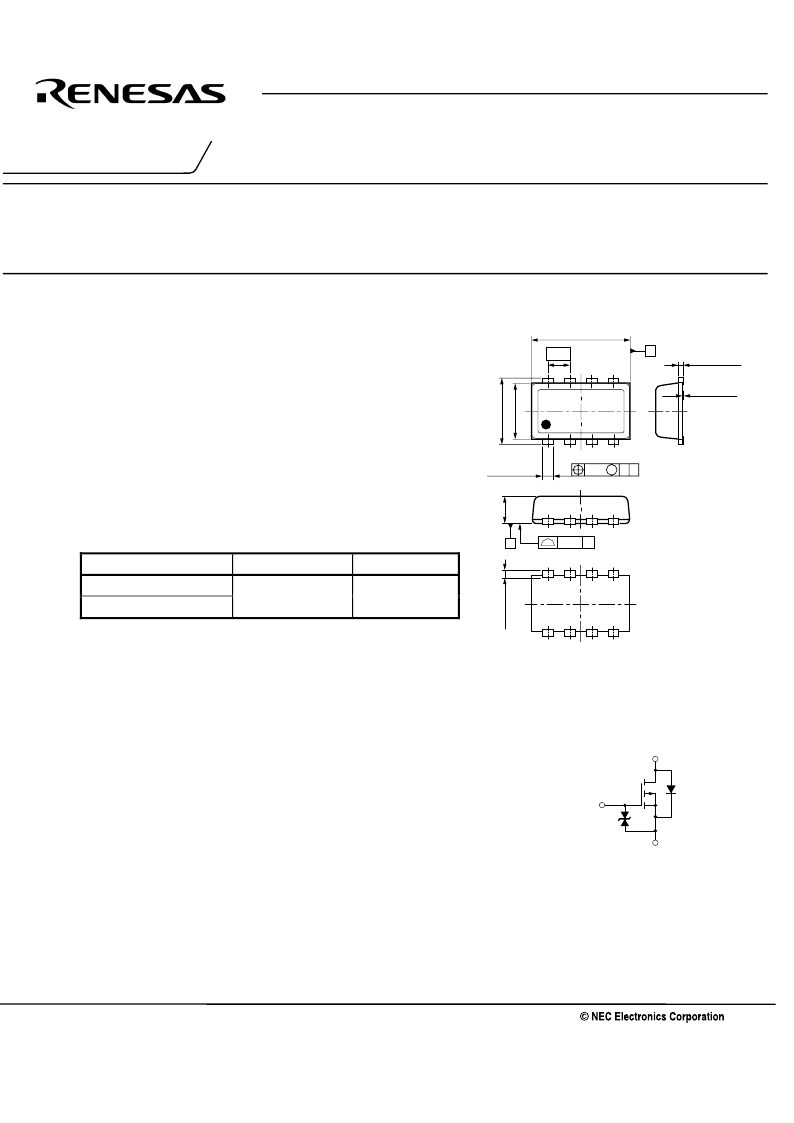
PACKAGE DRAWING (Unit: mm)
The μ PA2211T1M is P-channel MOS Field Effect Transistor designed
for power management applications of portable equipments, such as
load switch.
8
2.9 ± 0.1
0.65
5
A
0.145 ± 0.05
FEATURES
? Low on-state resistance
R DS(on)1 = 25 m Ω MAX. (V GS = ? 4.5 V, I D = ? 7.5 A)
0 to 0.025
R DS(on)2 = 34 m Ω MAX. (V GS = ? 2.5 V, I D = ? 3.8 A)
R DS(on)3 = 66 m Ω MAX. (V GS = ? 1.8 V, I D = ? 3.8 A)
? Built-in gate protection diode
? ? 1.8 V Gate drive available
ORDERING INFORMATION
0.32 ± 0.05
S
1
4
0.05 M S A
0.05 S
1, 2, 3, 6, 7, 8: Drain
4 : Gate
5 : Source
PART NUMBER
PACKING
PACKAGE
μ PA2211T1M-T1-AT
μ PA2211T1M-T2-AT
Note
Note
8 mm embossed taping
3000 p/reel
8-pin VSOF (1629)
0.011 g TYP.
Note Pb-free (This product does not contain Pb in external electrode and
other parts.)
ABSOLUTE MAXIMUM RATINGS (T A = 25 ° C, All terminals are connected.)
Drain to Source Voltage (V GS = 0 V)
Gate to Source Voltage (V DS = 0 V)
V DSS
V GSS
? 12
m 8
V
V
EQUIVALENT CIRCUIT
Drain Current (pulse)
Total Power Dissipation
Drain Current (DC)
Note1
Note2
Total Power Dissipation (PW = 5 sec)
Note2
I D(DC)
I D(pulse)
P T1
P T2
m 7.5
m 30
1.1
2.5
A
A
W
W
Gate
Drain
Body
Diode
Channel Temperature
Storage Temperature
Notes 1. PW ≤ 10 μ s, Duty Cycle ≤ 1%
T ch
T stg
150
? 55 to +150
° C
° C
Gate
Protection
Diode
Source
2. Mounted on glass epoxy board of 25.4 mm x 25.4 mm x 0.8 mmt
Remark The diode connected between the gate and source of the transistor serves as a protector against ESD. When
this device actually used, an additional protection circuit is externally required if a voltage exceeding the rated
voltage may be applied to this device.
The information in this document is subject to change without notice. Before using this document, please
confirm that this is the latest version.
Not all products and/or types are available in every country. Please check with an NEC Electronics
sales representative for availability and additional information.
Document No. G19452EJ1V0DS00 (1st edition)
Date Published September 2008 NS
Printed in Japan
2008
发布紧急采购,3分钟左右您将得到回复。
相关PDF资料
UPA2520T1H-T2-AT
MOSFET N-CH 30V VSOF
UPA2521T1H-T2-AT
MOSFET N-CH 30V VSOF
UPA2550T1H-T2-AT
MOSFET P-CH DUAL 12V 8VSOF
UPA2590T1H-T2-AT
MOSFET N/P-CH 30V 8VSOF
UPA2716AGR-E1-AT
MOSFET LV 8SOP
UPA2719AGR-E1-AT
MOSFET LV 8SOP
UPA2731UT1A-E1-AY
MOSFET P-CH 30V 8-HVSON
UPA2732UT1A-E1-AY
MOSFET LV 8HVSON
相关代理商/技术参数
UPA2350T1G-E4
制造商:Renesas Electronics Corporation 功能描述:
UPA2350T1P
制造商:RENESAS 制造商全称:Renesas Technology Corp 功能描述:MOS FIELD EFFECT TRANSISTOR
UPA2353
制造商:RENESAS 制造商全称:Renesas Technology Corp 功能描述:MOS FIELD EFFECT TRANSISTOR
UPA2353T1G-E4-A
制造商:RENESAS 制造商全称:Renesas Technology Corp 功能描述:MOS FIELD EFFECT TRANSISTOR
UPA2354
制造商:RENESAS 制造商全称:Renesas Technology Corp 功能描述:MOS FIELD EFFECT TRANSISTOR
UPA2354T1G-E4-A
制造商:RENESAS 制造商全称:Renesas Technology Corp 功能描述:MOS FIELD EFFECT TRANSISTOR
UPA2373T1P
制造商:RENESAS 制造商全称:Renesas Technology Corp 功能描述:Dual Drain common, N-channel MOSFET 24V, 6A, 23.0m
UPA2373T1P-E4-A
制造商:RENESAS 制造商全称:Renesas Technology Corp 功能描述:Dual Drain common, N-channel MOSFET 24V, 6A, 23.0m
